Design For TestabilityDFT experience in core and block level designs.

Design for Testability (DFT)As more and more transistors are shrunk into smaller and smaller area, accompanied by increase in design complexity, to sate the ever-increasing demands of the market, design for testability is indispensable in producing reliable, robust and high yield integrated circuit products. The addition of controllability & observability gives deep insight into the implementation of the design and allows rapid detection of manufacturing defects, root cause the issue and enables designers in identifying specific sections that need adjustment in order to meet reliability & yield targetsNeural Semiconductor has Design for Testability (DFT) experience in core and block level designs.

Our
Competency- DFT flow development and implementation both in core level and block level
- JTAG IEEE 1149.1, ACJTAG IEEE 1149.6 & IJTAG IEEE 1687
- DFT for mixed signal low speed and high-speed designs with multiple clock and voltage domains
- Expertise in Scan insertion
- Test Point Insertion, X bounding
- Boundary Scan, MBIST, LBIST
- Compression logic IP creation and synthesis (EDT, EDT Bypass)
- Gate Level Simulation (GLS)
- Automatic Test Pattern Generation (ATPG) & Coverage Analysis
- Pattern Simulation & Debugging
- Low Power ATPG & At-speed test
- Test data compression
- Post Silicon Diagnosis: Scan diagnosis, Layout Aware Diagnosis (LAD)
- Yield analysis test program development and production support
- Exposures in industry standard EDA tools: Mentor Graphics, Cadence
DFT Expertise
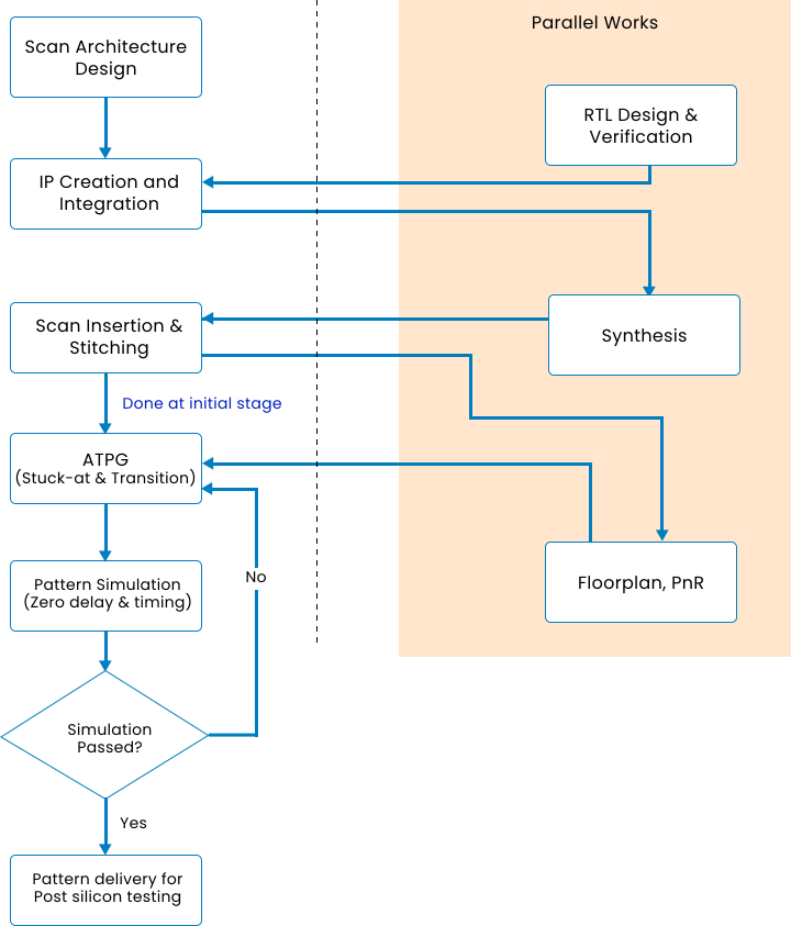
During the design phase, the DFT flow is started in parallel with RTL development, leveraging the DFT techniques to generate the minimum set of test vectors that guarantees the testability of all devices that will eventually be implemented. At pre-synthesis stage, DFT architecture is designed while in post synthesis, scan insertion is performed. Once successful, fault injection and pattern generation are done by targeting injected faults. Coverage analysis and pattern simulation with the scan inserted netlist is done to ensure that the generated patterns are ready before the design goes for fabrication. This ensures the efficacy of the generated test patterns in detecting the various faults at the physical level.
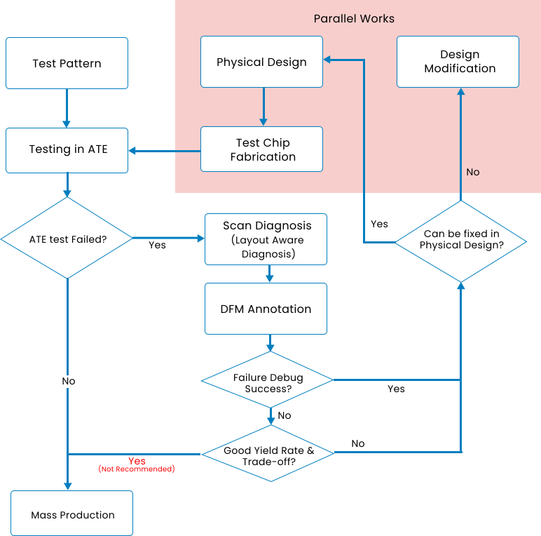
Before going to chip manufacturing, testing must be done to increase yield rate, avoid faulty chip production, and fine-tuning the fabrication process & fabrication environment using Automatic Test Equipment. ATE is a complex combination of both hardware and software. Hardware parts connect the test chips. With the help of the software, test patterns give stimuli to detect the presence of faults. If any test chip fails to pass the testing, ATE writes out a failure log. Our diagnosis & yield analysis team does 'layout-aware diagnosis' to find the fault sites, types, and density. After diagnosis and debugging, the yield & rejection rate ratio decides whether it will go for extensive production or design modification stages. The results from the analyses allow the design team to fix the issues at the physical design level and fabrication engineers to fine-tune the fabrication process. DFM annotation is also done at the post-silicon level to ensure the quality of mass production.
With the huge popularity of portable handheld and wearable devices, power consumption and product battery life has become a huge concern for today's design engineers. While designs incorporating low power techniques, such as multiple power domains, clock gating, dynamic voltage scaling and others, promises massive power savings, it has brought along its' own DFT challenges. Power aware scan chains and DFT techniques are employed for such designs to make sure the design remains testable even with the power reduction routines in place. Additional methodologies are also employed to reduce the power consumed by the test chip during ATE testing.